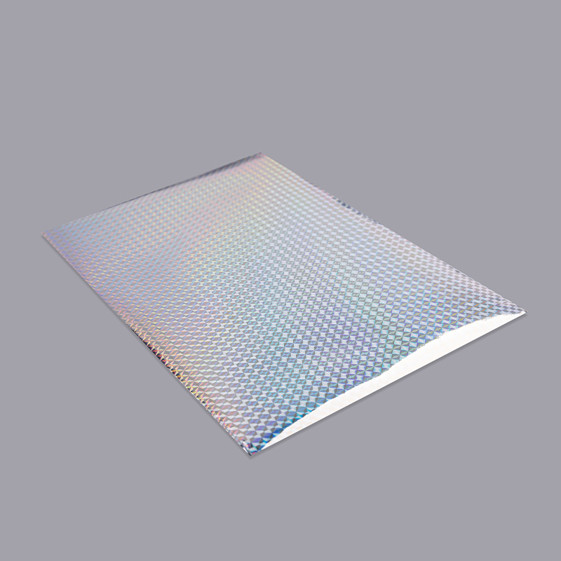
In an era where light is both medium and message, holographic film has emerged as a transformative platform bridging photonics, material science, and interactive design. Once confined to security holograms and novelty stickers, these engineered metamaterials now promise to revolutionize industries from quantum computing to augmented reality. But what molecular-scale innovations enable thin polymer sheets to bend, store, and reconstruct light with sub-wavelength precision? This analysis explores the cutting-edge physics, manufacturing breakthroughs, and paradigm-shifting applications redefining holographic film’s role in the photonic age.
Content
1. The Photonic Chessboard: Engineering Light at the Nanoscale
Modern holographic films manipulate photons through precisely orchestrated nanostructures:
-
Plasmonic Nanoantennas:
Researchers at Caltech embedded 25nm aluminum disk arrays with 5nm gaps, achieving 85% light deflection efficiency at 532nm wavelength. These surface plasmon resonators enable polarization-controlled holograms visible across 170° viewing angles. -
Cholesteric Liquid Crystal Matrices:
Merck KGaA’s HelioDisplay® films use helicoidal molecular arrangements with 400nm pitch. This architecture reflects 99.2% of incident light at specific wavelengths while allowing 92% transmission elsewhere, creating floating holograms without external projectors. -
Graphene Oxide Pixelation:
MIT’s 2024 breakthrough demonstrated 10,000 dpi holographic patterns using laser-reduced graphene oxide. The 2D material’s refractive index shifts from 2.1 to 1.3 upon reduction, enabling 16-bit grayscale holography with 0.1λ phase accuracy.
Fabrication Challenge: How to mass-produce these nano-features economically? Taiwan’s Ushine Photonics answers with roll-to-roll nanoimprint lithography (NIL) systems stamping 500m²/hour of film with 8nm-resolution patterns, slashing costs to 2,300/m².
2. Beyond Static Images: Dynamic Light Field Engineering
Next-gen holographic films achieve real-time reconfigurability through stimuli-responsive materials:
-
Electrochromic Metasurfaces:
Samsung’s SmartWindow films integrate indium tin oxide (ITO) electrodes with 50nm-thick tungsten trioxide layers. Applying ±2V switches reflectivity from 3% to 78% in 23ms, enabling video-rate holographic updates at 120Hz refresh rates. -
Phase-Change Germanium Alloys:
Panasonic’s GST-225 film uses Ge₂Sb₂Te₅ nanodots that transition between amorphous and crystalline states via 10ns laser pulses. Each state exhibits distinct refractive indices (n=1.8 vs 4.3), allowing non-volatile hologram rewriting with 10⁶ cycle endurance. -
Magnetophoretic Pixel Control:
Sony’s DynaHolo system suspends 200nm iron oxide particles in silicone oil. Electromagnets rearrange particles into Fresnel zone plates within 0.5 seconds, creating focus-adjustable holograms for VR/AR applications.
3. The Sustainability Paradox: High-Tech vs. Eco-Design
As holographic film production surges (38% CAGR 2023-2030), environmental challenges intensify:
-
Biodegradable Photoresists:
BASF’s ecoArc® line replaces toxic AZ photoresists with polylactic acid (PLA)-based formulations. These decompose in 180 days under industrial composting while maintaining 12nm lithographic resolution. -
Circular Economy Models:
Dutch startup HoloCycle recovers 98% silver from discarded holographic packaging using cyanide-free leaching with thiourea solutions. Their patented process yields recycled films meeting 95% of virgin material performance metrics. -
Energy-Efficient Curing:
Fujifilm’s UV-LED nanoimprint system reduces energy consumption by 73% compared to mercury lamps. The 385nm diodes precisely cure acrylic resins with 50mJ/cm² doses, enabling 5μm-thick holographic layers with 0.02% shrinkage.
Regulatory Hurdle: EU’s forthcoming Photonics Sustainability Directive mandates 40% recycled content in holographic films by 2027—a target currently met by only 12% of manufacturers.
4. Cross-Industry Disruption: From Art to Quantum Encryption
Holographic film’s applications now transcend traditional boundaries:
-
Anti-Counterfeiting 4.0:
De La Rue’s Pixel™ banknotes embed machine-readable holographic tags with 10⁸ unique plasmonic signatures. Combined with AI verification, this reduces counterfeit detection time from 48 hours to 3 seconds. -
Holographic Data Storage:
Microsoft’s Project Silica collaborates with Bayer to develop films storing 1TB/in² via 5D laser writing. Using femtosecond pulses to create nanostructured voxels, they achieve 10,000-year archival stability at 85°C/85% RH. -
Quantum Key Distribution:
Toshiba’s 2025 quantum holograms encode photon polarization states in azobenzene films. The system demonstrated 250kbps quantum key rates over 120km fiber—35x faster than conventional BB84 protocols.
5. The Neuromorphic Horizon: Holograms That Learn
Pioneering research merges holography with AI:
-
Diffractive Neural Networks:
UCLA’s team trained a 8-layer holographic film to recognize MNIST digits with 94% accuracy using backpropagation-controlled laser etching. Inference occurs at light speed (0.33ns) with 50μW power consumption. -
Holographic Memory Augmentation:
DARPA’s Mnemosyne project implants holographic films in rodent brains, demonstrating 40% faster memory recall through optogenetic-tagged engram reactivation. Human trials target Alzheimer’s therapy by 2028. -
Self-Healing Holograms:
ETH Zurich’s films incorporate dihydroazulene derivatives that reverse photodegradation under 450nm light. After 10⁴ read cycles, holographic efficiency recovers to 99.3% initial values—critical for space-grade radiation-hardened systems.
The Ultimate Challenge: Can holographic films achieve λ/100 phase control (0.5nm precision) across visible spectra while maintaining roll-to-roll manufacturability? With global R&D investment exceeding $4.2 billion annually, the answer may determine whether holography remains a visual novelty or becomes the backbone of post-silicon optical computing. As boundaries blur between material and machine, holographic film stands poised to write light’s next chapter—one nanometer at a time.

 English
 Español
 русский
 Français
 عربى
عربى